

Transmission line explorations
Transmission line explorations
An trip across the jungle of microstrip lines at high speed

When you start a high speed design at rates and/or with trace lengths higher that those of you comfort zone is very useful to make some investigations about the terrain you have to move on, which are the actuating knobs you have and the influence of each of them.

Conditions of the study
In this post of today we are going to explore differential transmission lines for a hypothetical PCIe Gen3 system. This standard has a transmission rate of 8 Gbps per lane. We are going to use a trace distance of 20 cm (8 inches): this is an arbitrary but reasonable distance that adds some precision to the analysis.
The differential transmission lines will be defined for a target differential impedance of 85 Ω, which is the recommended value for connector interface. PCIe requirements are quite relaxed in this respect.
We will make the study only for microstrip lines because most of this type of circuits use this structure.
We will use a PCB stackup in which the dielectric layer has a thickness of 116.8 μm, a typical value for 6 layer PCB.
We assume a continuous and uninterrupted ground plane.
For all the study (but the last step) evaluated dielectric will be FR4 (and in particular FR408HR) that has an specification of dielectric constant (DK) of 3.22 and dielectric loss (DF) of 0.011, them all at 5 GHz. However, this precise data varies on where you look. One reason for that is that the dielectric has some frequency variability.
Solder mask: we will consider a default coating with 30 μm thickness and a dielectric constant of 4.2. In the study we will evaluate its influence.
Copper thickness will have a reference height of 1/2 oz/inch^2, which is the standard one used for high density boards. This is equivalent to 17.8 μm.
Copper roughness will have the standard value of 6 μm.
For the study we will use Polar Si9000 Transmission Line Field Solver (commercial tool) and Sierra Circuits (free online tool available in this link). The results provided by them are quite coherent but Polar provides losses graphs that give a lot of insight.
Methodology
We will study (in this order):
In differential pairs, we have a freedom degree: the level of coupling between the two traces of the pair. We will see how this will influence the physical dimensions of the traces and the signal attenuation (losses). We will make a decision and we will continue our analysis based on that.
We will analyze the influence of dielectric manufacturing thickness.
We will analyze the influence of the solder mask (manufacturing tolerance).
We will analyze the influence of the copper thickness.
We will analyze the influence of the trace etching shape.
We will analyze the influence of the copper roughness.
We will analyze the influence of the PCB dielectric.
We will end with a summary and conclusions.
Such study could be much wider and include the effect of using striplines, the effect of the serial capacitors that such a system requires, the usage of exotic materials. Maybe in a future post we will dare with these and even more aspects.
Differential transmission lines, are they so different?
Almost everybody knows that high speed design has an strong requirement of controlling characteristic impedance.
The characteristic impedance of a single ended transmission line is characteristic of it, depends on on how is build.
However, when we have a differential transmission line, all this magic disappear: the propagation depends not only on the pair construction but on the type of signals it carries. To make the story short, we study two different propagation modes and each of them has a different impedance and propagation speed. These modes are called even (for a common mode signal) and odd (for a pure differential signal with no common mode). We will use the expression differential impedance but we should more properly make reference to odd impedance. Strictly speaking, differential impedance is twice odd impedance. The expression differential impedance has become the common term used in the industry.
While impedance control is essential to tame reflections and get the best signal integrity, loss control is also of extreme importance when we use lossy media, which becomes relevant when the data rate is high or the trace length is great.
Cables and traces have a very nice characteristic: high frequency attenuation tends to follow a linear law with frequency. This means that we can see losses in two complimentary ways: as a problem of attenuation at high frequency or as a problem of reduced bandwidth. This is something that deserves a more deeper and detailed analysis in a future post.
All previous discussion can be summarized in a very simple idea: we have to pay attention to impedance match but also to signal attenuation in the way to know how much we have and where does it come from.
Let's start the party!
The effect of coupling
In the first step of the exploration analysis, we will compare the coupling effect of the lines in the differential pair. We will move between two extremes: from placing the traces a distance of 100 μm (which is a the typical minimum distance for very dense circuits that the PCB manufacturers guarantee) to 500 μm, in which the coupling is so loose that we can (almost) see the pair as two single ended transmission lines in which the differential impedance is twice the single ended characteristic impedance of one of the lines.
Figure below shows that as pair traces separates, the width of each one has to increase to keep differential impedance constant but this increases saturates towards two single ended transmission lines, as explained before.

Next figure shows the losses.
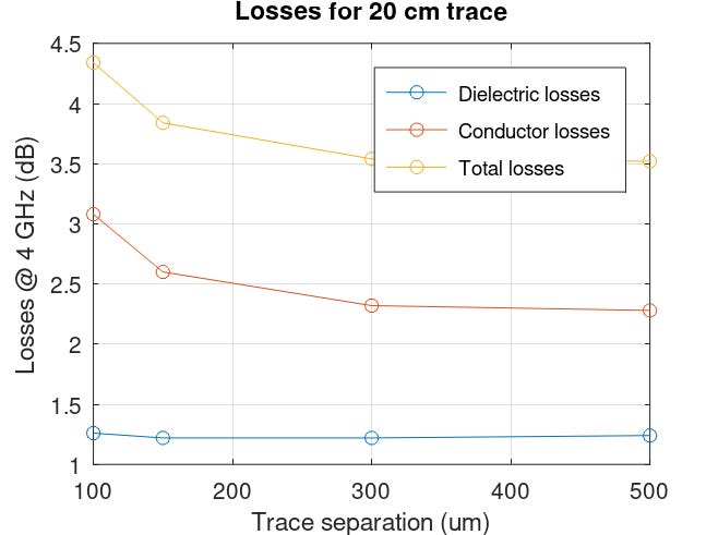
This figure shows something we could expect: as trace width increases, there is a significant reduction of copper losses. There is a very slight increase in the dielectric looses, as more width means that more field has to propagate across the isolator.
We see that for all scenarios, the losses figures are relatively low. A loss of 4.3 dB at Nyquist frequency means that the signal amplitude will be reduced by a factor of 0.6 in optimum sampling point, which is negligible. A rule of thumb is that you don't need extra measures if losses are under 8 dB. We have large margin.
When losses are not a limiting factor, the most adequate option is to use as thigh coupling as possible. This means that for the rest of the study, we will consider a trace separation (S1) of 100 μm and a trace width (W1) of 192 μm.

The influence of the dielectric thickness
One PCB manufacturer specifies that dielectric thickness is 116.8 ± 18 μm.

We can see that this tolerance produces about ±5% variation in differential impedance (-4.8, +3.7 Ω). This is something can can be a bit painful for some applications (not too much for this one).
The influence of the solder mask
Solder mask thickness is not controlled in the manufacturing process as well as other parameters despite it has significant influence for high speed applications.
With the field solver we will calculate which is the influence of having no solder mask at all. We configure it as a solder mask made of air, with a dielectric constant of 1.0.
We see that in this extreme situation, the characteristic impedance of the pair increases 12 Ω (a 14 %). This figure is not like previous one, we do not have the risk of having no solder mask at all, but shows that you need to ask the PCB manufacturer which is the possible thickness range and evaluate it.
Removing solder mask slightly reduces the losses because in the air there is no losses, and also very small improvement in copper losses which I cannot explain. Having no solder mask in the 20 cm trace produces an improvement of less that 0.7 dB.
Influence of the copper thickness
The copper thickness is typically well controlled if the PCB manufacturer does not increase it with a galvanic process.
We will consider an standard copper thickness of 0.5 oz/inch^2 and we will calculate the change of impedance when it varies ±10 %. The result is a mere ±1 % change in Zdiff. However, in conversation with Lab Circuits, they have reported me that via metallization requires a significant increase in copper thickness. Be aware of that.
The losses change are quite small. While increasing the copper thickness slightly reduces the conductor losses, the skin effect dominates the effective section in which the current flows. But expect higher Zd increment if trace thickness is higher.
The total loss variation is lower that 0.3 dB in the 20 cm of traces length.
Influence of the trace etching
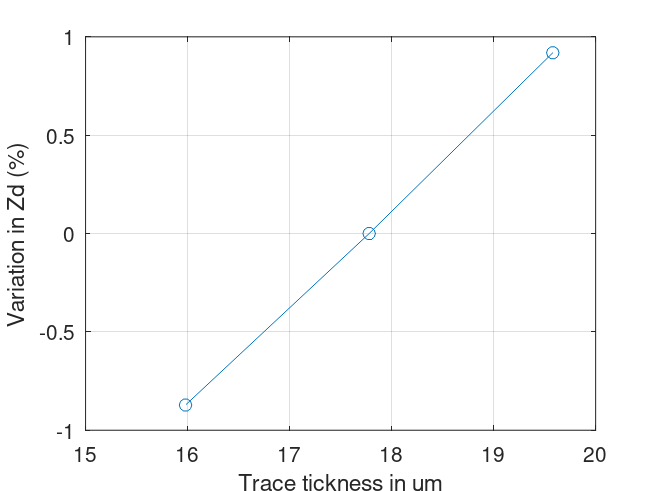
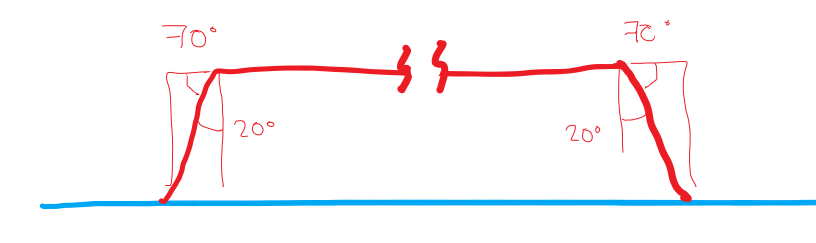
In this simulation we want to evaluate another manufacturing tolerance. For time being we have considered that the trace section is rectangular, ideal. However, in practice the section is trapezoidal, with an angle of 70 º. This reduces the upper trace width from W1 of 192 μm to 187 μm.
In this circumstance, the differential impedance of the line increases 1.1 Ω (which is very low) while attenuation variation is absolutely marginal.
Influence of the copper roughness
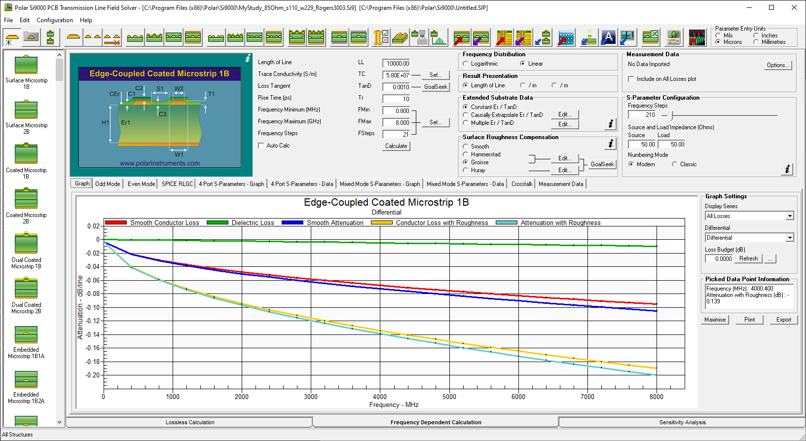
There is a surprising effect at high frequency: the conductor losses are quite higher than those predicted by the conductor resistivity and skin effect. The investigations revealed that there is an extra effect due to the copper roughness: the rougher the copper the is, the more the conductor losses are. And not in an small quantity.
The standard copper roughness is 6 μm. The following figure shows the losses for a very low profile copper, that reduced the roughness by half (to 3 μm).
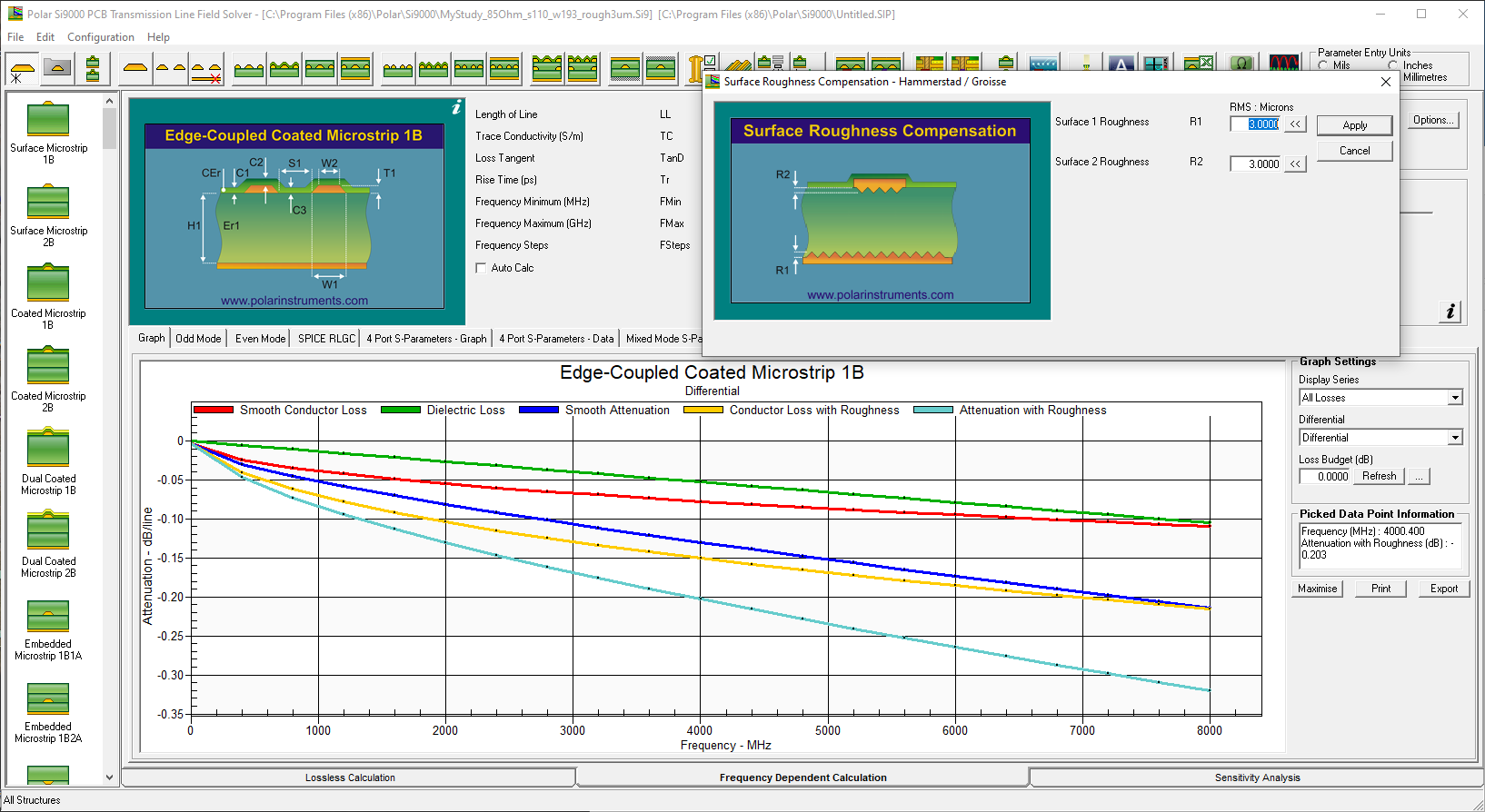
The lower part of the shows attenuation by centimeter between DC and 8 GHz. The plot requires an explanation:
Dielectric loss (in green) shows the losses in the dielectric. Shown value is for FR4.
Smooth conductor loss (red color) shows losses for copper conductivity and skin effect: that is, ideally smooth metal.
Smooth attenuation (blue) is the total loss for smooth copper, combination of the previous parameters.
Conductor loss with roughness (beige) shows the losses with actual copper roughness (which can be calculated with different models, not visible in the screen)
Attenuation with roughness (cyan) is the total loss with actual copper roughness, combination of the dielectric loss and the conductor loss with roughness.
The improvement of the conductor loss is not much. A mere 0.003 dB/cm. While copper roughness has its influence, it is quite small.
Change in the dielectric material
The FR4 (flame retardant number 4) is by far, the mostly used material for PCB manufacturing. It is a very good compromise between cost, electrical performance and mechanical robustness. In previous figures we have seen that dielectric loss tends to have relatively low impact in final losses but conductor losses are part of the Laws of Nature and reduction of copper roughness does not allow great improvement.
For our application (PCIe Gen3), FR4 is a very nice option but we may have others with higher data rate and/or trace lengths in which the most practical way to improve losses is by using a high performance dielectric. Needless to say that this will impact cost.
The last part of the experiment is done feeding the field solver with other materials.
The first experiment was done with Rogers RO4003C, which has a dielectric constant of 3.4 (very stable value up to 10 GHz) and low dissipation factor (DF) of 0.004.
First point to notice is that a change in the dielectric constant requires a change of trace width (W1) a reduction to 184 μm. Total loss improvement is about 0.8 dB for 20 cm trace.
However, if we use a Rogers RO3003 dielectric, based on PTFE (Teflon), dielectric loss virtually vanishes. The result is shown in the next figure. This improvement is not justified for our application but may be pure gold for others.
Summary and conclusions
We have been exploring different scenarios for a could-be application of PCIe Gen3, which has a Nyquist frequency of 4 GHz.
We have evaluated different coupling options and while tight coupling produces more losses that a loose one, absolute values show we can support it without further enhancements. At the same time, this solution makes optimum use of board space and minimum crosstalk for equal wiring density.
The effect of dielectric thickness or solder mask thickness in characteristic impedance is quite significant, but has minor effect on losses. This is of secondary importance in our application but may justify ordering impedance control in the PCB manufacturing process (see this post).
The variation of copper thickness has small influence in characteristic impedance and also in losses. Discuss with PCB manufacturer what they can guarantee you in this respect.
The effect of etching imperfections can be neglected both in terms of characteristic impedance and losses.
The effect of copper roughness has some effect in conductor losses but not very much and the impact in complexity is large.
There are dielectric materials that can reduced the losses in a very significant amount to the point of making the conductor losses (almost) the single contributor. Be aware that changing the material implies changing trace geometry and may influence in may other aspects: worth having a detailed analysis to all the factors involved in selection of dielectric materials.
For high speed transmission both control of characteristic impedance and losses is important. Most systems accepts variations of characteristic impedance of 5 % and many allow 10% variations. Beyond that you have to do a very careful analysis.
The summary of the summary is that for systems similar to the one studied, good engineering practices combined with a precise PCB manufacturing should lead to trouble free designs, but both are a must.
As this post length has duplicated the typical reading time of 5 minutes, next week there will be no newsletter.