


Manufacturing PCBs with controlled impedance
What's that? Does it make sense?

When an engineer has to manufacture a RF or high speed digital circuit, the PCB manufacturer may ask if the PCB requires control of impedance. This is a service that implies an extra cost, which means that needs to be well understood and justified.
Photo by Dan Lohmar on Unsplash
What's trace impedance?
When a PCB works at DC, the only thing you have to care about your traces is its resistance.
When the signal frequency rises you may have to take into account trace inductance, and even mutual inductance between traces or current loops. The whole trace can be precisely modeled by a couple of discrete components.
However, when the bandwidth of the signals rise even more, we have to move from a lumped or discrete element model to a transmission line or distributed model. This happens when the signal transition time is comparable to the time the signal takes to propagate across trace length.
When the signal source makes such a fast transition, the transmission line behaves as a low value resistor than requires continuous supply of current while the signal propagates across trace length. The value of this resistance is the one of the characteristic impedance of the line, also called Z0. The Z0 depends on the geometry of the traces and the effective dielectric constant that the electromagnetic field sees.
When do you need controlled impedance of the PCB traces?
When an engineer designs a board knows if it has to model it using transmission line model or the lumped model is good enough.
When I have a high speed design, I start with a conversations with the PCB manufacturer and we make an agreement about the board stackup and I ask for the dielectric constant of the materials used. With this information, I calculate with great care trace widths and distances between pairs if the design involves differential pairs.
If the PCB manufacturer ask me if I want impedance control, the obvious question could be: «Are you telling me that you cannot control your PCB process? Can trace impedance be uncontrolled?».
However, the question is reasonable. A transmission line impedance depends on many factors (in decreasing importance):
The trace width. There is a rule of thumb that says that a microstrip line made with FR4 dielectric, a 50 Ω trace requires a width that is about two times the dielectric thickness. A 75 Ω requires a trace width that is about dielectric thickness.
The dielectric material thickness.
The effective dielectric constant (DK) of the space in which the electromagnetic field propagates (mixture of air and PCB dielectric in a microstrip line, just PCB dielectric in a stripline structure).
The trace copper thickness.
The trace section geometry which in practice tends to be a bit trapezoidal.
When we design a trace in the CAD, we conceive a perfect trace of copper. However, we need to know that this trace is manufactured with a well controlled chemical process, which is subject to tolerances and imperfections: trace width is not going to be absolutely uniform across length. Worth remember that the trace widths we use in typical high speed circuits could be about 150 μm (5 mils).
Depending on the number of layers of the PCB, the manufacturer has to use different laminate materials. For certain layers, they use one called prepreg, that need to be compressed during manufacturing. Once again, this process has certain tolerance.
The most typical material we use for PCB dielectric is FR4 (Fire Retardant number 4). It is made of a mixture of glass fiber fabric and epoxy. These two materials have very different dielectric constants (DK of 6 and 3.5 respectively) and even in the best controlled manufacturing process there is some DK dispersion.
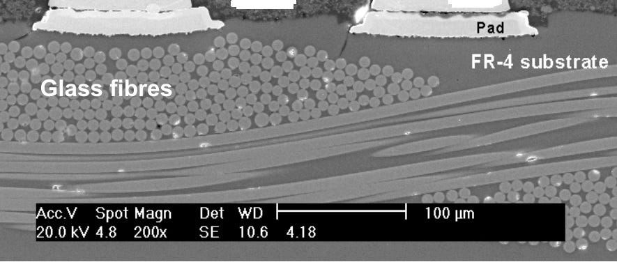
(Photo shows a section of a PCB. You can see the glass fibre fabric)
To make things more complicated, the dielectric constant of FR4 has some dependency with frequency and temperature.
While reputed PCB manufacturer uses high quality material and has a precise control of the manufacturing process, the nature has its limits. Also different products have different tolerance to dispersion of the the characteristic impedance (Z0) of traces.
Measuring characteristic impedance
Worth mentioning that PCBs are manufactured in large panels, in which there are many instances of every individual PCB. In order to measure the effective trace impedance, the manufacturer will add certain patters (coupons) that contain relatively long transmission lines with the desired characteristic impedance. Coupons contain traces in any relevant layer.

Photo courtesy of Lab Circuits - See vertical test coupons at both sides of the PCB
Later on, when the PCB is manufactured, the quality control team measure the impedance of coupon lines and compares against the specification. If the impedance value measured is outside limits, the boards in the same production panel will be rejected and not delivered to you.
The technique used is called Time Domain Reflectometry (TDR) which is able to measure the impedance of a line across its length.
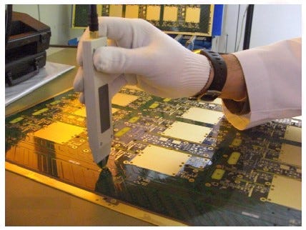
Photo courtesy of Lab Circuits - Measuring coupons
The typical acceptance range for Z0 variation is ±10%. If needs to be tighter, the cost will increase.
Cost implications
It can be easily understood that this process has some cost implications:
It involves very complex and costly instrumentation and also coupon generation techniques.
Requires manual testing of various coupons in every PCB panel.
May involve scrapping of boards, and thus increase of the number of manufactured boards or reduction of its delivered number.
As coupons take space, there may be penalty in the number of boards that can be placed in a panel.
Final advice is to have a very sincere conversation with your PCB manufacturer and eventually order an small run of controlled impedance boards. This order should include the measurement reports in which you will be able to see the actual values and its dispersion in the batch.

Photo courtesy of Lab Circuits - Controlled Z certificate