


How good conductors are copper traces?
All that glitters is not gold


The resistance of PCB traces
Once I had to deal with a board that had a problem because the trace resistance was much higher than expected and the I·R drop1 in the traces exceeded specifications.
Indeed, it is very convenient to have an idea of how good conductors PCB traces are. I bet they are less good than you may think!
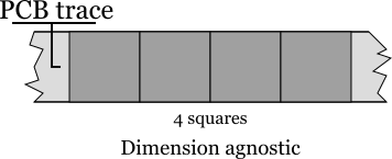
The side-to-side resistance of an square conductor is independent of its size: thick about it and you will understand. This means that a trace resistance is proportional to the number of squares it contains!
Copper thickness is traditionally measured in terms of weight. A reference value is 1 oz/ft^2. (We say this copper has 1-ounce). For those of us that are used to SI units, this is equivalent to 35 μm thickness.
The resistivity of a square of copper of 1-oz at 25 ºC is 500 μΩ. Multiply by 1.5 at 125 ºC. Divide by two for 2-oz copper; multiply by two for 0.5-oz copper.
Trace resistance is proportional to the number of squares it contains.
The resistivity of a square of copper of 1-oz at 25 ºC is 500 μΩ.
Examples for 1-oz copper:
A trace which is 5 mil wide, 50 mil long contains 10 squares, and thus have a resistivity of 5 mΩ. This is a short between two pins in a 100-mils spacing device (after a typical discount of crowns over pads).
A 0.2 mm trace width and 100 mm long contains 500 squares, and thus have 250 mΩ.
Calculating trace widths
When you have to carry large currents across PCB traces, you have to take into account two aspects:
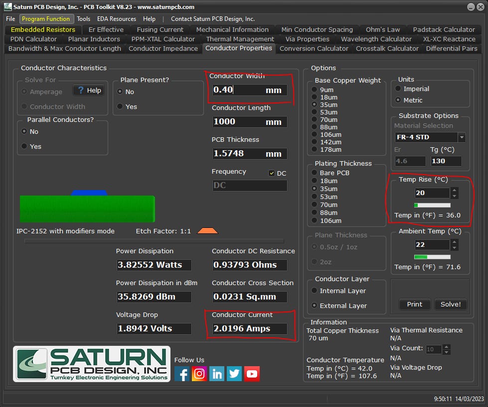
Self heating, which also increases copper resistance. Self heating is not length dependent. There is a IPC recommendation about it (IPC-2152). However, I have always used tools like SaturnPCB (link) that allows you to calculate it easily instead of dealing with tables.
IR drop, which is length dependent.
Imagine that we need a trace to support 2.0 A for a PCB of 35 µm (1-oz) copper thickness. We will calculate minimum trace width for copper temperature increase of 20 ºC (which is quite standard). SaturnPCB (say IPC-2152) recommends a minimum trace width of 0.40 mm. [This value is for an isolated track: if the current return path is close, the current capability will be strongly reduced. The tool also supports it: for two traces, ampacity reduced by half].
What can I do to increase current flow?
One approach to increase current capability is to use 2-oz in external layers but you have to request it specifically to the PCB manufacturer. This has a cost increase and beware that typically is not compatible to very dense boards. Beware that that the chemical processes than can make traces thicker have relatively poor repeatability. I suggest to have a conversation with your PCB manufacturer to transit this way.
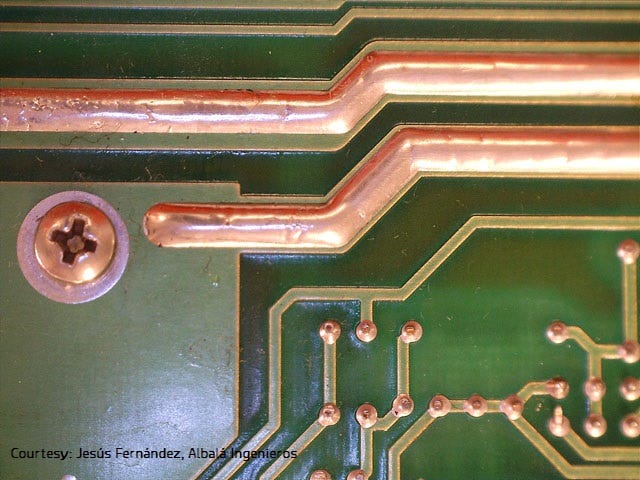
Some high power PCAs use a trick to increase trace section: flood the trace with tin. It is a way to gain some margin when all other approaches are not possible. Next figure is taken from a real product, a PSU. It has one half the resistance of the PCB trace. Copper thickness is 110 μm (3.2-oz obtained by plus extra chemical). Sn-Pb alloy has 9 times the copper resistivity.
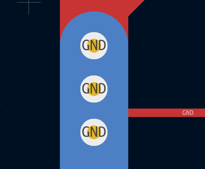
The via to high current is not only a good trace
When you need high currents, traces are only one part of the challenge. If we need to change the trace layer we need a via.
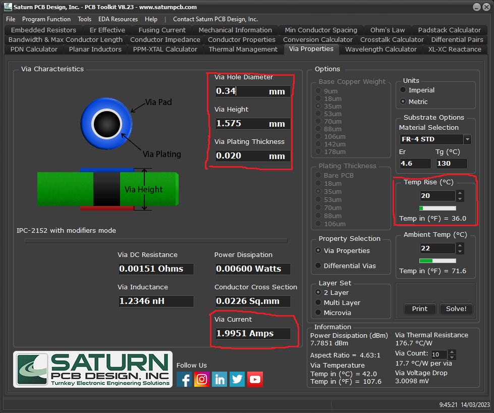
When investigating data from a quality local PCB manufacturer (Lab Circuits), they report a mean plating thickness of 25 µm and 20 µm minimum. I will use this latter figure for a conservative design. For a side to side via, SaturnPCB recommends a (minimum) drill diameter of 0.34 mm for a via current of 2.0 A. Via DC resistance is 1.5 mΩ. It sounds low and it is low: it is equivalent to 3 copper squares.
However, when current requirements are higher, the via diameter has to grow to impractical values. The solution is to place various vias in parallel to increase alternative current paths. This is especially true in a real PCB with many other traces that also carry large amounts of current. An beware that traces in internal layers have large more difficult to dissipate heat.
While modern CAD tools offer the unique capability to make very detailed analysis of IR drop and temperature increase, rules of thumb are an excellent way to orientate a design.
By I·R drop, we mean the voltage drop due to Ohm’s Law