
Clock and data recovery
The Clock and Data Recovery is a PLL that is able to extract the timing information from a data stream. It is used in very large number of communication interfaces like PCIe, USB, SGMII.


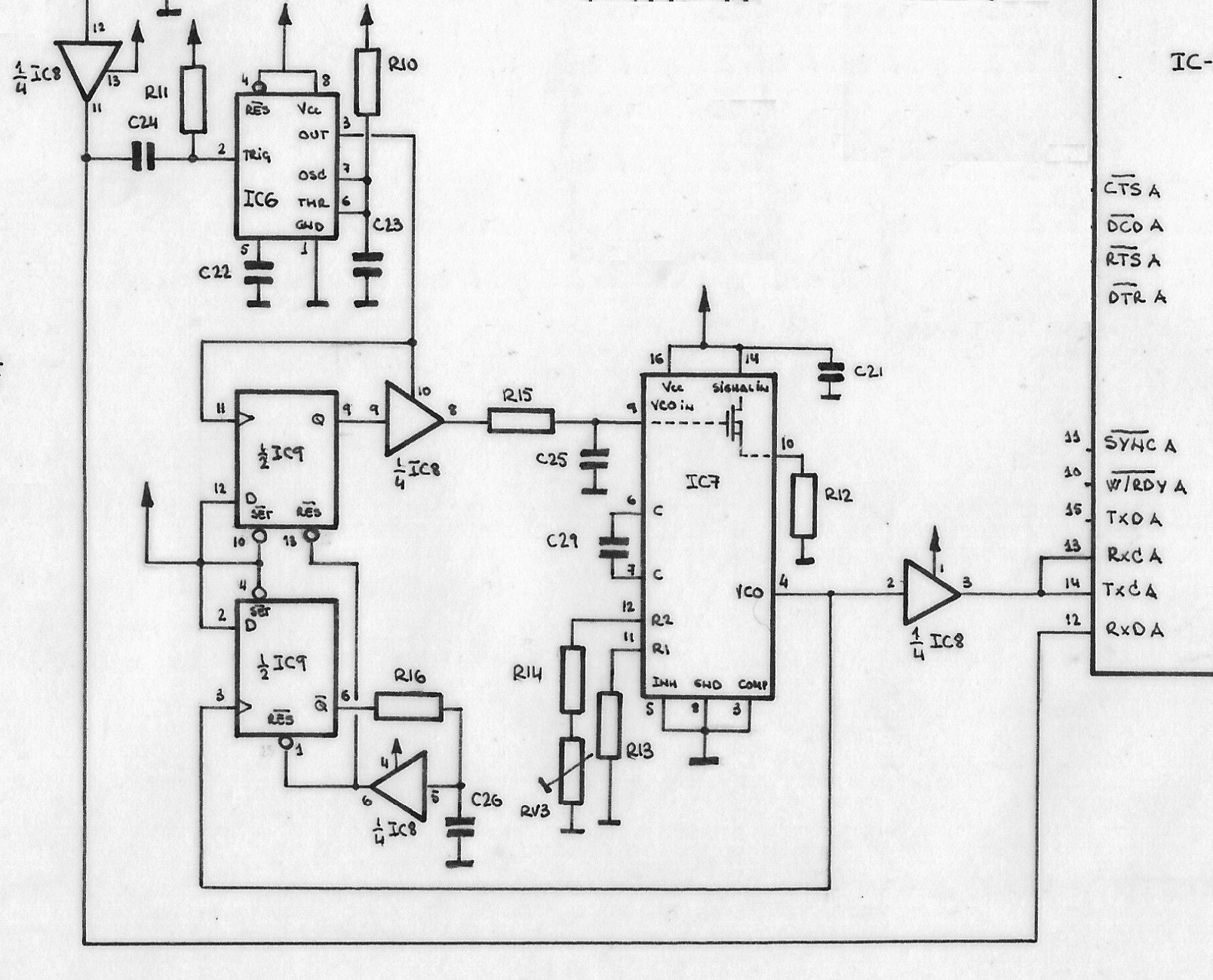
While searching my archives for photographs for this newsletter, I made an unexpected discovery: the electrical diagram of my Master’s Thesis in Engineering. It was 1988 and it was very nicely hand drawn in onion paper with India ink.
I wanted to share with you the Clock and Data Recovery (CDR) section in its original format.
Background
The CDR system is a PLL in which the VCO has to synchronize in phase with the received data in order to sample it in its optimum sampling point, which for bandwidth limited signals, is the time between data transitions. If you prefer it, data transitions are better aligned with clock falling edges.
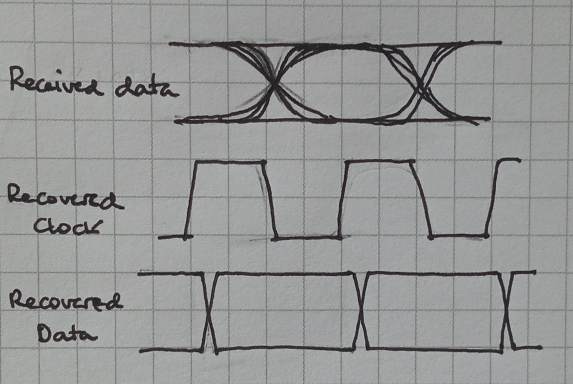
However, we should remember that the data to recover is random in nature and there is no logical state transitions in every transmitted bit, but randomly at fixed intervals.
It should be noticed that the PLL phase comparator can provide phase correction information only when there is data state transition (may be rising or falling).
This is why in this kind of interfaces a line code is introduced. In my project was 6B8B, while a very typical one is 8B10B. This means that if I wanted to transmit a 6-bits word. I transmitted a 8-bit one. In 6-bits words there are 32 possible combinations and in an 8-bit word, 256. This means that the protocol designer has to select among 256 combinations the 32 better ones in terms of data transitions. For example 0x00 and 0xFF have to be purged from the table. I remember that I did this this code sieve work partially automatically, partially by hand. It was 1988 and there was not an standard for 6B8B and is more than likely there will never be!
How does it work
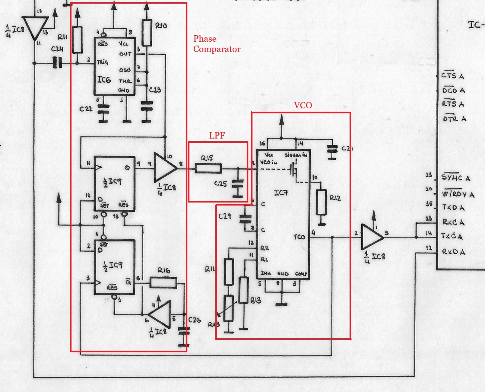
Phase comparator uses:
A monostable with a period of a bit, IC6. It is triggered by a data rising edge.
Two flip-flops (IC9). We will see its operation in few lines
A triestate buffer, IC8. When there is information, the ouput is high or low but when there are no useful data transitions, remains in high impedance, not correcting VCO control voltage.
To complete the PLL, we have IC7 PLL and R15, C25 loop filter.
Phase comparator operation
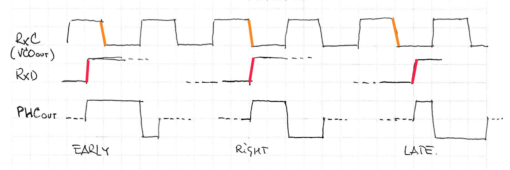
By default, the two flip-flops are in reset state. This means that Q is 0 and nQ is 1.
A data transition1 triggers IC6 monostable. This produces two effects. First, sets upper flip-plop Q output to high logical level. Second, puts IC8 buffer in low impedance: high logical level (if we neglect transients).
Later on, a VCO rising edge will come. This will set the lower flip-flop setting nQ output to low level. R16 by C26 time constant should be very short and after a very small delay, nRES becomes low (active) and the two flip-flops will reset. This sets triestate buffer low level while the bit period lasts.
In the figure that follows we can see the phase comparator output when data arrives early, just in time (aligned with clock falling edge) and late.
The low pass filter smooths phase comparator output and is the responsible of locking speed and the loop stability (never forget it is a closed loop).
Improvements
Looking at it now, I see some flaws in the design. Nevertheless, the CDR I designed from scratch worked flawlessly in recovering a clock for an optical communication system.
Later on, I used similar approaches for recovering low noise, 2 Mbps satellite signals with very low signal to noise ratio and also digital video links at ~300 Mbps. These new implementations did not require the analog monostable and took information from both data edges (very convenient). This implies sacrificing linearity of the phase comparator, which is not a practical problem.
These newer implementations used VHDL code and do not have the beauty of the circuit’s drawing I have shared with you today.
In this circuit, just a rising edge data transition. It misses half the available information, which is also in the falling edges.