
Using Transient Voltage Supressors
This post introduces to the selection and use of ESD (Electro Static Discharge) protection devices, also called Transient Voltage Suppressors (TVS), a name that is not very fortunate.


The evils of over-voltages
Probably you have observed that it you touch a ground connected equipment after walking over a carpet, you get a very small ark. The arc is the product of an over-voltage that is able to make the air to conduct electricity when the electrical field is sufficiently high.
The consequences of over-voltages over semiconductor devices are:
instantaneous damage of the device (destruction) when the energy is high (IC trace blow up, perforation of isolation barriers),
progressive degradation of the devices if energy is not high enough to destroy it immediately,
latch-up, where too much current flows from the power supply after a transient over-voltage.
Failures due electrical over-voltages is one of the most significant causes of electronic board malfunction.
Over-voltage transients
Electronic equipment cannot be designed and tested using people that walk over carpets and touches the device under test (DUT). Instead of that, there are international standards that establish test conditions that the equipment have to resist without failure. Among them, the most important is IEC-61000-4-2 (level 4).
It is reasonable to think that if a board is compatible with this standard, it is going to be very robust in the field if used inside buildings. We not include lightning effects.
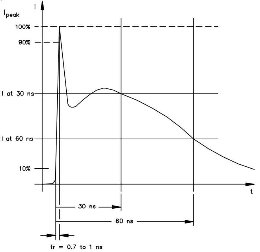
Please observe that the pulse is defined in terms of electrical current.
Two important parameters of these transients are:
Its energy, that needs to be absorbed somewhere,
Its rise time, related to transient bandwidth.
Typically, ICs are built with ESD protection diodes that are compatible to Human Body Model (HBM) and Charge Device Model (CDM). However, for higher energy discharge (like IEC-61000-4-2, level 4) there is need of external (larger silicon area) devices that are able to dissipate higher energy pulses.
Selecting ESD protection devices
Transient voltage suppressor (TVS) devices are Zener diodes with large PN unions to allow large current density spikes. They have the drawback of being be very capacitive. However, there are new devices/architectures that can be very protective while reducing the capacity load to the circuit.
Device type and parameters
If we consider the electrical transfer function, we find two types of TVS devices:
Unidirectional: transfer function is like a Zener diode. Use them for analog and digital unipolar lines.
Bidirectional: symmetrical transfer function. Use for analog and digital bipolar lines (like RS232) and many differential signaling systems (like CAN, RS422, RS485) that should work with positive and negative common mode voltages.
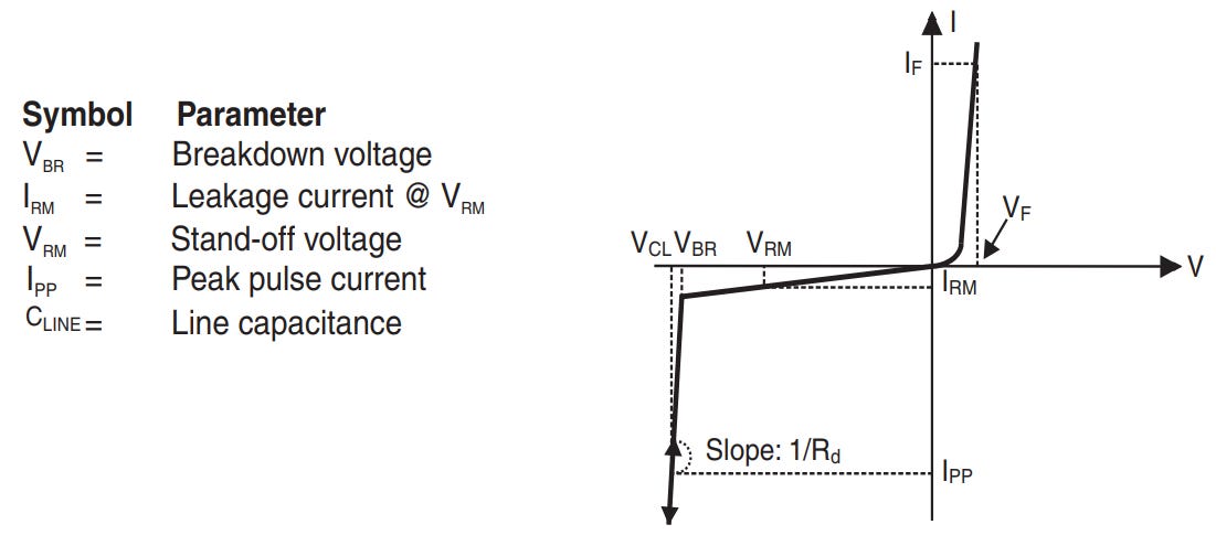
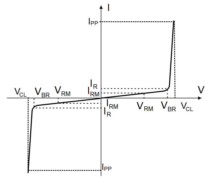
Them all are characterized by three regions. The most essential parameters are shown in bold:
No influence region: Working Peak Reverse Voltage (Vrwm or Vrm) at Maximum Reverse Leakage current (Irm). In this region, the device should be as transparent as possible.
Breakdown, the transition point in which the diode starts operating: Breakdown voltage (Vbr) at Test Current (It). This parameter is the less relevant of the group.
Clamping: Clamping Voltage (Vcl) at Peak Pulse Current (Ipp).
It worth notice that for the same family of devices, the product Vcl⋅Ipp is constant: it is related to the device capability of power dissipation.
Device implementation
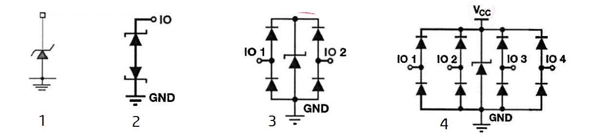
There are four possible device implementations. They establish behavior and also influence capacity load.
Fast transient protection diode. Zener-like diode, unidirectional. High capacity.
Two opposite zener diodes. Bidirectional. Mid capacity.
Transient protection device + diodes. Low capacity.
Biased transient protection device. Ultra Low capacity.
How the TVS diode protects
We need to think in TVS diodes as shock reduction devices not as fully absorption one: under the presence of a shock, the device conducts current and absorbs part of the energy.
They are the first barrier against the attack. Inside the device we want to protect there use to be protection diodes. We may need another intermediate barrier between the EDS protection and the final device, but this is out of scope in this post.
In next figure we see the testing environment, the voltage of the tester without the protection device (reaching 8 kV in open circuit) and the voltage obtained after the clamping device (300 V peak, much lower energy). Vertical scale is very relevant.
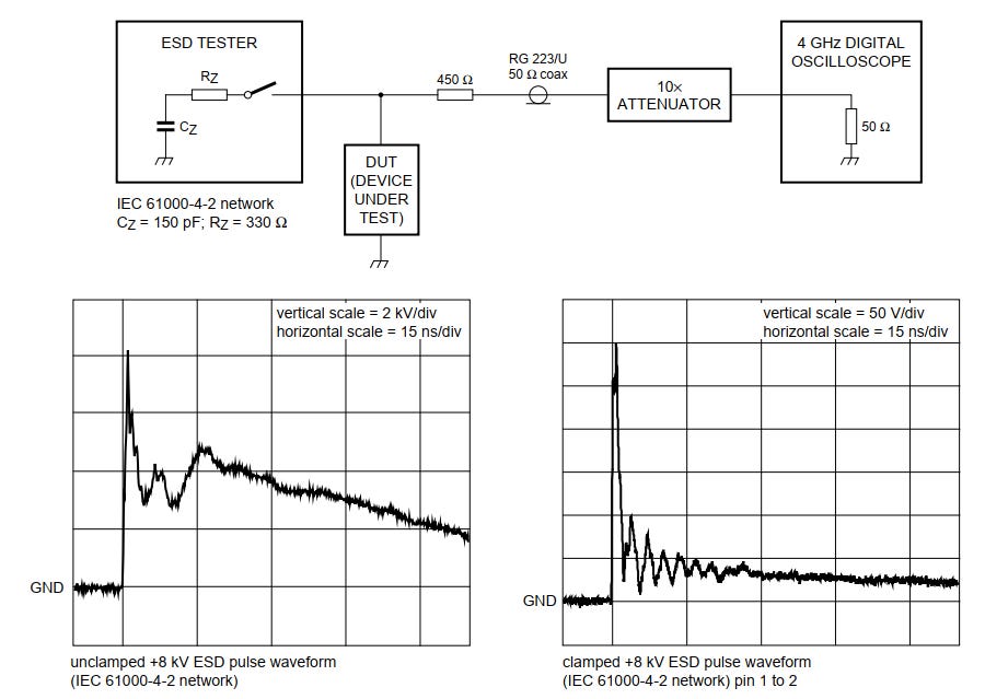
It becomes clear that the term suppressor is not very fortunate.
Layout of ESD diodes
Placing diodes does not solve by itself the ESD problems.
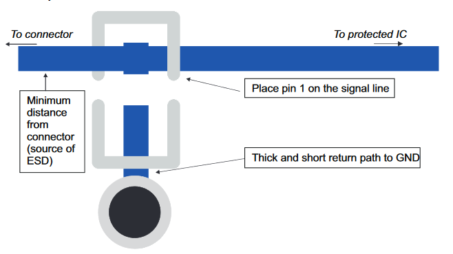
We need to place them in the right way.
The ESD pulse bandwidth is close to 500 MHz. It is essential to minimize the inductance of the traces in series with the ESD protection device that is seen by the device to protect. Otherwise, the large and fast current spike will produce a big voltage drop in the trace and the voltage seen by the device to protect will rise accordingly.
Let us make some back of the envelope calculations for a wrongly routed signal. Imagine that he circuit to protect see in the path of current discharge a TVS diode in series with 1 cm of PCB trace. A 50 Ω transmission line over FR4 has a distributed inductance of 3.3 nH/cm. As current variation for IEC 61000-4-2 level-4 is 30 A/ns, the voltage drop in the inductance equivalent to 1 cm trace will be 100 V (V = L⋅dI/dt). The ’protected’ input will see the clamping at the device plus 100 V.
Inductance can be minimized by shorter and thicker traces, thick via hole and by placing extra vias.
Summary and conclusions
ESD protection devices should be used in the lines that interfaces the external world,
ESD protection devices should be properly selected to offer protection and not to disturb signals,
For the protection to be effective, layout should be cared because ESD events have very high bandwidth.
Sorry for being longer that 3 minutes reading time. I was unable to condense it more.