


Chopper amplifiers: history and present
A closer look to this fascinating technique


The chopper amplifier is one of the techniques used to obtain ultra low offset amplifiers (see a past column of this newsletter) that comes from the ancient ages of electronics.
Valve amplifiers had terrible performance for amplifying DC or low frequency signals but the use of feedback changes the game. Negative feedback (one of the greatest inventions of the century) makes the gain dependent on the relationship of values of a pair of passive components and not the amplifier itself. The idea behind a chopper amplifier is to chop a DC-low frequency signal and convert it to an AC symmetrical one, them amplify it with very well controlled gain, and then demodulate back to DC. The result is the removal of most of the (large) DC offset of the amplifier and its low frequency noise (1/f), being both things very important for large gain amplifiers.
Oldies but goodies
A good example of that is the Hewlett Packard 410C valve voltmeter which is able to measure DC voltage, DC current, resistance and AC voltage up to 700 Mc (in 1963, when the meter reached the market, was common to measure frequency in Mc, Mega-cycles). Measuring it in Hertz came later. Link to the User Manual. Meter amplifiers were based on thermionic valves.
The block diagram, taken from the User Manual is gorgeous.
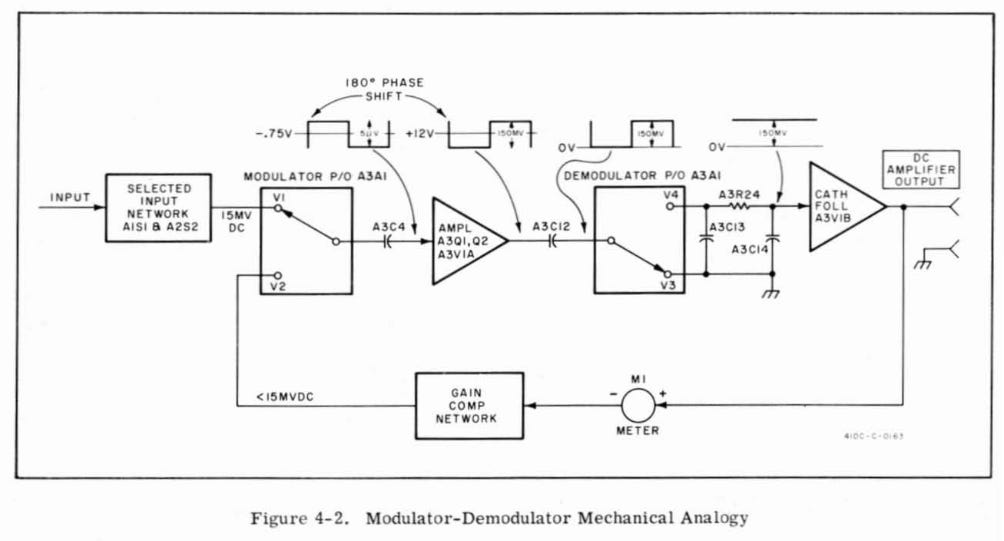
At that time, HP did a great improvement replacing electro-mechanical switches (relays) by solid state devices, which greatly improves meter reliability. The solution was really brilliant (pun intended): the chopping was done optically, using cadmium sulfide (CdS) light depending resistors (LDR) who has a very high resistance value in the darkness and is quite conductive when illuminated. Light comes from a relaxation oscillator that drives two neon lamps that operate in counter phase. Earlier instruments used mains synchronous motors that set chopper frequency to 5/6 of the mains frequency to avoid aliasing with the ever present mains components that degrade output measurement. Neon lamps have much longer life that incandescent bulbs.
Contemporary implementation
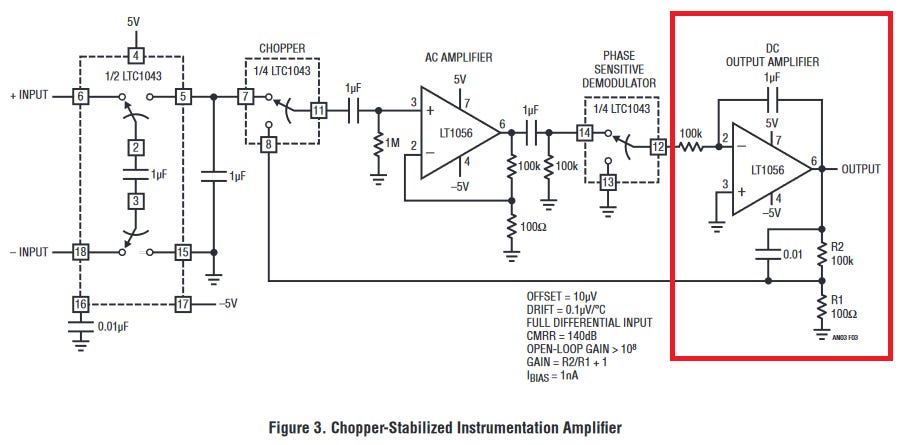
Jim Williams, while working for Linear Technology, wrote an application note AN3 Applications for a Switched-Capacitor Instrumentation Building Block (Link). In it, appears this Ultrahigh Performance Instrumentation Amplifier which has some similitude to HP-410C block diagram and which may be easier to follow for a contemporary engineer.

In the diagram itself we can read that the gain is 1001 (R2/R1+1) and the superb amplifier offset (10 μV) and its drift (0.1 μV/ºC).
How it works
This circuit is a master piece of engineering and works generating an AC signal with the error signal. The error signal is the difference between the differential input voltage and amplifier's output attenuated by the feedback factor (R1 and R2 voltage divider).
It surprises me when someone says something like «Electronics bore me, because I have already learned it all». It is impossible to have blood in the brains and seeing the circuit we present today without a feeling of wonder and admiration.
Negative feedback
Next figure shows a generic system with negative feedback.

A fraction of the output signal is subtracted from the input and amplified. The resulting closed loop gain Acl, is mostly dependent of the feedback factor ( β ) and not of open loop gain (Aol).
If loop gain ( β·Aol) is much greater that one, we can simplify and we get:
With this in the memory, let us see how circuit works.
Astounding common mode rejection
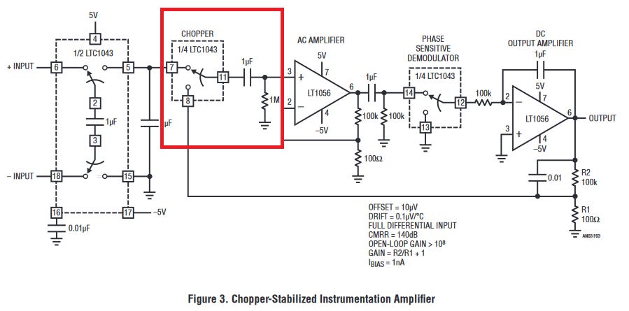
The differential input voltage charges the capacitor that is placed between pins 2 and 3 of the LTC1043. When switches to the right, transfers its charge to the ground referenced capacitor, who has equal capacity. This input stage produces an astounding common mode rejection (limited only by asymmetrical leakage) , but in a way that is unrelated to the chopper principle.

Chopping
When looking at the multiplexer datasheet, I could see that the capacitor between pin 16 and ground sets switching frequency. For 10 nF, we get the lowest specified one, a chopping frequency of about 500 Hz.
We will distinguish two phases, that we are going to call A and B. Let us call A the phase in which the switches are in the position drawn in the schematic and B the other. There is a mistake in the drawing of the schematic in the section labeled as phase sensitive demodulator, not in the circuit itself: in Phase A, the pins 12 and 13 are shorted. I will keep the original drawing except for the output stage in which I will correct it.
Output
Let us start from the beginning: let us have a look to the output stage :-)
The last stage is a pure integrator followed by a voltage divider that sets the amplifier gain (β, the feedback factor).
A pure integrator, when seen in the frequency domain, can be seen as a low pass filter. It has very large gain at DC (the op amp open loop gain) and decreasing gain as frequency increases. Unity gain frequency is 1.6 Hz.
The output integrator will try to reach a voltage which is 1001 times the input one. That is, after transient settling, the voltage after the R1 and R2 divider (pin 8) will be equal to the input voltage (pin 7).
1.3.5 First chopper stage
The voltage at pin 11 of the LTC1043 (the error signal) will be:
Phase A: Input voltage
Phase B: Output voltage after the voltage divider formed by R1 and R2.
When the output is settled, we will have a very low amplitude signal. While settling we will have a signal whose peak to peak amplitude is the error voltage, with its corresponding sign.
This 500 Hz square signal is offered to a first order high pass signal formed with a R of 1 MΩ and a capacitor of 1 μF. This has a cutoff frequency of 0.16Hz, more that 3 decades under fundamental frequency of the signal. This means that the RC filter will just remove DC component but will not distort the square wave: it will just shift it around 0 V.
AC amplifier
The 'AC amplifier' will boost the signal with a gain of 1001 V/V, set by the ratio of its feedback resistors. The gain is positive: there is no signal inversion. The DC offset of the opamp will also be amplified by this gain but will be blocked by the next AC coupling.

Output reconstruction - Phase sensitive demodulator
At pin 14 of the LTC1043 once again we will have a symmetrical AC signal whose peak to peak amplitude will be 1001 times the error voltage. It will be a signal that is very similar to an square one.
During phase A, the input of the integrator will be at 0 V. Due to virtual ground principle, ideally, the two outputs of the amplifier will be at ground potential. In practice, the inverting input will have the offset voltage, but this will be strongly attenuated by the feedback. No current will flow across the 100 K input resistor and thus, output voltage will not change

In phase B, the integrator will see half the amplitude of the the error signal. Any voltage different from zero will produce a slow voltage ramp the output amplifier in the opposite direction of the error signal.
Step response
Let us see what happens if we have a constant input voltage of 1 mV and the integrator capacitor (1 μF) is discharged.
The signal at the AC amplifier will have an amplitude of 1 mV peak to peak and its output will have an amplitude of 1.001 V peak to peak.
In reference to the integrator:
During phase A, the integrator will remain at 0 V output.
During phase B, current will begin to low across the integrator R and C. Current will be 5 μA. This will produce a ramp of growing voltage. At the end of the semi-cycle, it will be:
This means that the output amplifier reacts trying to follow the positive input, as corresponds to a negative feedback amplifier.
Stability
Today's article has been longer than usual and we still have not analyzed the stability of the circuit.
In a future post we will remember the stability criteria of a negative feedback amplifiers and the magic of those that have integrators in their the open loop gain.